Categories
  • Pin Configurable/Selectable Oscillators(8,248)
View Mode:result_1_0result_1_1result_2_0result_2_1
Email

Leave Us A Message!

We`re not around but we still want to hear from you! Leave us a note:

SEND
EmailWhatsApp
*You can contact us directly on WhatsApp!
  • img

    DSA2033FL2-F0012TVAO

    100 LVDS X 2, -40-105C, 25PPM

    Microchip Technology

  • img

    DSA612NL1A-01UKTVAO

    3-OUTPUT MEMS AUTOMOTIVE CLOCK G

    Microchip Technology

  • img

    DSC6122HE1B-022M

    MEMS OSC. (FS), ULTRA LOW POWER,

    Microchip Technology

  • img

    DSA613RL2A-0200TVAO

    3-OUTPUT MEMS AUTOMOTIVE CLOCK G

    Microchip Technology

  • img

    DSA613NA2A-01V6TVAO

    3-OUTPUT MEMS AUTOMOTIVE CLOCK G

    Microchip Technology

  • img

    DSA613RA3A-020CVAO

    3-OUTPUT MEMS AUTOMOTIVE CLOCK G

    Microchip Technology

  • img

    DSA612RL2A-0232VAO

    3-OUTPUT MEMS AUTOMOTIVE CLOCK G

    Microchip Technology

  • img

    DSA612PI3A-021MTVAO

    3-OUTPUT MEMS AUTOMOTIVE CLOCK G

    Microchip Technology

  • img

    DSC6021HA2B-020M

    MEMS OSC, LVCMOS, FREQ SELECT, 2

    Microchip Technology

  • img

    DSA612PA1A-01GCVAO

    3-OUTPUT MEMS AUTOMOTIVE CLOCK G

    Microchip Technology

  • img

    DSA613NA2A-01WDTVAO

    3-OUTPUT MEMS AUTOMOTIVE CLOCK G

    Microchip Technology

  • img

    DSA613NA2A-01WDVAO

    3-OUTPUT MEMS AUTOMOTIVE CLOCK G

    Microchip Technology

  • img

    DSA612RA2A-023YTVAO

    3-OUTPUT MEMS AUTOMOTIVE CLOCK G

    Microchip Technology

  • img

    DSA612RL3A-0132VAO

    3-OUTPUT MEMS AUTOMOTIVE CLOCK G

    Microchip Technology

  • img

    DSA613PL3A-01WMTVAO

    3-OUTPUT MEMS AUTOMOTIVE CLOCK G

    Microchip Technology

  • img

    DSA2044FL1-F0022VAO

    100 HCSL X 2, -40-105C, 50PPM

    Microchip Technology

  • img

    DSA612RL3A-0132TVAO

    3-OUTPUT MEMS AUTOMOTIVE CLOCK G

    Microchip Technology

  • img

    DSA2021FL1-F0014VAO

    100 LVPECL X 1, 100 LVCMOS X 1,

    Microchip Technology

  • img

    DSA612RL2A-0232TVAO

    3-OUTPUT MEMS AUTOMOTIVE CLOCK G

    Microchip Technology

  • img

    DSA612RL3A-01YYTVAO

    3-OUTPUT MEMS AUTOMOTIVE CLOCK G

    Microchip Technology

  • Total 5000
    • 1
    • 2
    • 3
    • 4
    • 5
    • 6
    • 250

    What is a pin configuration/selectable oscillator?

    A pin configuration/selectable oscillator refers to the layout and positioning of the metal pins or terminals on an electronic component, enabling connections to other components or a printed circuit board. The pin configuration is essential because it dictates how the component can be connected to other parts and how it fits into a circuit design.
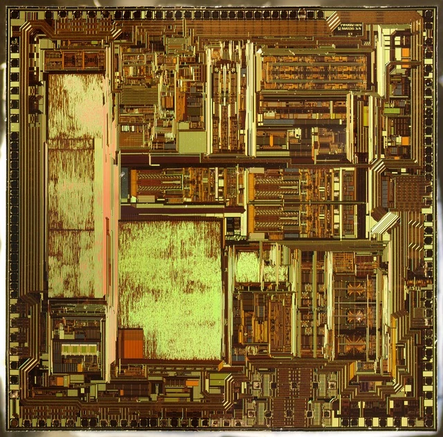
    A pin configuration/selectable oscillator


    How to read a Pin Configuration Diagram?

    A pin configuration diagram, often referred to as a pinout diagram, visually illustrates the pins or terminals of an electronic component along with their functions. Understanding how to interpret this diagram is crucial when working with electronic components. Here are the steps to follow:


    A pin configuration diagram,


    Step 1: Identify the Component

    Start by identifying the electronic component you need to reference. The component's name and part number will typically be found on the datasheet.


    Step 2: Locate the Pin Configuration Diagram

    Find the pin configuration diagram within the datasheet. It may be labeled as “Pinout,” “Pin Configuration,” or “Pin Connection Diagram.”


    Step 3: Identify the Pin Numbering

    The pin numbering assigns a unique identifier to each pin or terminal. Generally, the pins are numbered sequentially, beginning with pin one and progressing upwards. The numbers may be shown next to each pin or within the pin box in the diagram.


    Step 4: Identify the Pin Functions

    Each pin serves a specific purpose, and the pin configuration diagram will outline these functions, often indicated by labels next to the pins or inside the pin boxes. Some pins may have multiple functions, which will be noted with various labels.


    Step 5: Identify the Pin Placement

    Pin placement refers to the physical location of each pin on the component. The diagram may include an illustration or image of the component with each pin clearly labeled and numbered.


    Step 6: Determine the Pin Connections

    After identifying the pin functions, numbering, and placement, you can ascertain how to connect the component within the circuit. The diagram will indicate which pins need to be connected to other components or the circuit board.

    Filters
    ApplyReset All
    • Manufacturers
    • Stocking Options
    • Environmental Options
    • Height
    • Voltage - Supply
    • Type
    • Spread Spectrum Bandwidth
    • Size / Dimension
    • Ratings
    • Package / Case
    • Output
    • Operating Temperature
    • Operating Mode
    • Mounting Type
    • Load Capacitance
    • Height - Seated (Max)
    • Absolute Pull Range (APR)
    • Function
    • Frequency Tolerance
    • Frequency Stability
    • Frequency - Output 4
    • Frequency - Output 3
    • Frequency - Output 2
    • Frequency - Output 1
    • Frequency
    • ESR (Equivalent Series Resistance)
    • Current - Supply (Max)
    • Base Resonator
    Attribute column